Extended IO operation functions. More...

Functions | |
| HAL_StatusTypeDef | HAL_FLASHEx_Erase (FLASH_EraseInitTypeDef *pEraseInit, uint32_t *SectorError) |
| Perform a mass erase or erase the specified FLASH memory sectors. | |
| HAL_StatusTypeDef | HAL_FLASHEx_Erase_IT (FLASH_EraseInitTypeDef *pEraseInit) |
| Perform a mass erase or erase the specified FLASH memory sectors with interrupt enabled. | |
| HAL_StatusTypeDef | HAL_FLASHEx_OBProgram (FLASH_OBProgramInitTypeDef *pOBInit) |
| Program option bytes. | |
| void | HAL_FLASHEx_OBGetConfig (FLASH_OBProgramInitTypeDef *pOBInit) |
| Get the Option byte configuration. | |
| HAL_StatusTypeDef | HAL_FLASHEx_AdvOBProgram (FLASH_AdvOBProgramInitTypeDef *pAdvOBInit) |
| Program option bytes. | |
| void | HAL_FLASHEx_AdvOBGetConfig (FLASH_AdvOBProgramInitTypeDef *pAdvOBInit) |
| Get the OBEX byte configuration. | |
| HAL_StatusTypeDef | HAL_FLASHEx_OB_SelectPCROP (void) |
| Select the Protection Mode. | |
| HAL_StatusTypeDef | HAL_FLASHEx_OB_DeSelectPCROP (void) |
| Deselect the Protection Mode. | |
| uint16_t | HAL_FLASHEx_OB_GetBank2WRP (void) |
| Returns the FLASH Write Protection Option Bytes value for Bank 2. | |
| HAL_StatusTypeDef | HAL_FLASHEx_Unlock_Bank1 (void) |
| Unlock the FLASH Bank1 control registers access. | |
| HAL_StatusTypeDef | HAL_FLASHEx_Lock_Bank1 (void) |
| Locks the FLASH Bank1 control registers access. | |
| HAL_StatusTypeDef | HAL_FLASHEx_Unlock_Bank2 (void) |
| Unlock the FLASH Bank2 control registers access. | |
| HAL_StatusTypeDef | HAL_FLASHEx_Lock_Bank2 (void) |
| Locks the FLASH Bank2 control registers access. | |
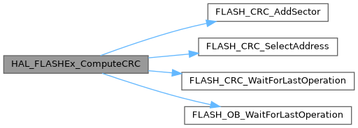
| HAL_StatusTypeDef | HAL_FLASHEx_ComputeCRC (FLASH_CRCInitTypeDef *pCRCInit, uint32_t *CRC_Result) |
Detailed Description
Extended IO operation functions.
 ===============================================================================
                ##### Extended programming operation functions #####
 ===============================================================================
    [..]
    This subsection provides a set of functions allowing to manage the Extension FLASH
    programming operations.
===============================================================================
##### Extended programming operation functions #####
===============================================================================
[..]
This subsection provides a set of functions allowing to manage the Extension FLASH
programming operations Operations. Function Documentation
◆ HAL_FLASHEx_AdvOBGetConfig()
| void HAL_FLASHEx_AdvOBGetConfig | ( | FLASH_AdvOBProgramInitTypeDef * | pAdvOBInit | ) |
Get the OBEX byte configuration.
- Parameters
-
pAdvOBInit pointer to an FLASH_AdvOBProgramInitTypeDef structure that contains the configuration information for the programming.
- Return values
-
None
Definition at line 482 of file stm32f4xx_hal_flash_ex.c.
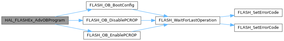
◆ HAL_FLASHEx_AdvOBProgram()
| HAL_StatusTypeDef HAL_FLASHEx_AdvOBProgram | ( | FLASH_AdvOBProgramInitTypeDef * | pAdvOBInit | ) |
Program option bytes.
- Parameters
-
pAdvOBInit pointer to an FLASH_AdvOBProgramInitTypeDef structure that contains the configuration information for the programming.
- Return values
-
HAL Status
Definition at line 430 of file stm32f4xx_hal_flash_ex.c.
◆ HAL_FLASHEx_ComputeCRC()
| HAL_StatusTypeDef HAL_FLASHEx_ComputeCRC | ( | FLASH_CRCInitTypeDef * | pCRCInit, |
| uint32_t * | CRC_Result | ||
| ) |
Definition at line 708 of file stm32h7xx_hal_flash_ex.c.
◆ HAL_FLASHEx_Erase()
| HAL_StatusTypeDef HAL_FLASHEx_Erase | ( | FLASH_EraseInitTypeDef * | pEraseInit, |
| uint32_t * | SectorError | ||
| ) |
Perform a mass erase or erase the specified FLASH memory sectors.
- Parameters
-
[in] pEraseInit pointer to an FLASH_EraseInitTypeDef structure that contains the configuration information for the erasing. [out] SectorError pointer to variable that contains the configuration information on faulty sector in case of error (0xFFFFFFFF means that all the sectors have been correctly erased)
- Return values
-
HAL Status
Definition at line 190 of file stm32f4xx_hal_flash_ex.c.

◆ HAL_FLASHEx_Erase_IT()
| HAL_StatusTypeDef HAL_FLASHEx_Erase_IT | ( | FLASH_EraseInitTypeDef * | pEraseInit | ) |
Perform a mass erase or erase the specified FLASH memory sectors with interrupt enabled.
- Parameters
-
pEraseInit pointer to an FLASH_EraseInitTypeDef structure that contains the configuration information for the erasing.
- Return values
-
HAL Status
- Parameters
-
pEraseInit pointer to an FLASH_EraseInitTypeDef structure that contains the configuration information for the erasing.
- Return values
-
HAL Status
Definition at line 261 of file stm32f4xx_hal_flash_ex.c.

◆ HAL_FLASHEx_Lock_Bank1()
| HAL_StatusTypeDef HAL_FLASHEx_Lock_Bank1 | ( | void | ) |
Locks the FLASH Bank1 control registers access.
- Return values
-
HAL Status
Definition at line 655 of file stm32h7xx_hal_flash_ex.c.
◆ HAL_FLASHEx_Lock_Bank2()
| HAL_StatusTypeDef HAL_FLASHEx_Lock_Bank2 | ( | void | ) |
Locks the FLASH Bank2 control registers access.
- Return values
-
HAL Status
Definition at line 689 of file stm32h7xx_hal_flash_ex.c.
◆ HAL_FLASHEx_OB_DeSelectPCROP()
| HAL_StatusTypeDef HAL_FLASHEx_OB_DeSelectPCROP | ( | void | ) |
Deselect the Protection Mode.
- Note
- After PCROP activated Option Byte modification NOT POSSIBLE! excepted Global Read Out Protection modification (from level1 to level0)
- Once SPRMOD bit is active unprotection of a protected sector is not possible
- Read a protected sector will set RDERR Flag and write a protected sector will set WRPERR Flag
- This function can be used only for STM32F42xxx/STM32F43xxx/STM32F401xx/STM32F411xx/STM32F446xx/ STM32F469xx/STM32F479xx devices.
- Return values
-
HAL Status
Definition at line 537 of file stm32f4xx_hal_flash_ex.c.
◆ HAL_FLASHEx_OB_GetBank2WRP()
| uint16_t HAL_FLASHEx_OB_GetBank2WRP | ( | void | ) |
Returns the FLASH Write Protection Option Bytes value for Bank 2.
- Note
- This function can be used only for STM32F42xxx/STM32F43xxx/STM32F469xx/STM32F479xx devices.
- Return values
-
The FLASH Write Protection Option Bytes value
Definition at line 558 of file stm32f4xx_hal_flash_ex.c.
◆ HAL_FLASHEx_OB_SelectPCROP()
| HAL_StatusTypeDef HAL_FLASHEx_OB_SelectPCROP | ( | void | ) |
Select the Protection Mode.
- Note
- After PCROP activated Option Byte modification NOT POSSIBLE! excepted Global Read Out Protection modification (from level1 to level0)
- Once SPRMOD bit is active unprotection of a protected sector is not possible
- Read a protected sector will set RDERR Flag and write a protected sector will set WRPERR Flag
- This function can be used only for STM32F42xxx/STM32F43xxx/STM32F401xx/STM32F411xx/STM32F446xx/ STM32F469xx/STM32F479xx devices.
- Return values
-
HAL Status
Definition at line 512 of file stm32f4xx_hal_flash_ex.c.
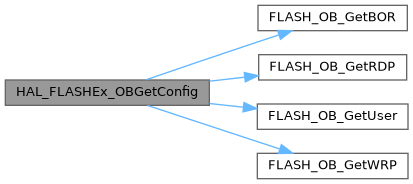
◆ HAL_FLASHEx_OBGetConfig()
| void HAL_FLASHEx_OBGetConfig | ( | FLASH_OBProgramInitTypeDef * | pOBInit | ) |
Get the Option byte configuration.
- Parameters
-
pOBInit pointer to an FLASH_OBInitStruct structure that contains the configuration information for the programming.
- Return values
-
None
- Parameters
-
pOBInit pointer to an FLASH_OBInitStruct structure that contains the configuration information for the programming.
- Note
- The parameter Banks of the pOBInit structure must be set exclusively to FLASH_BANK_1 or FLASH_BANK_2, as this parameter is use to get the given Bank WRP, PCROP and secured area configuration.
- Return values
-
None
Definition at line 402 of file stm32f4xx_hal_flash_ex.c.
Referenced by BOR_Get().

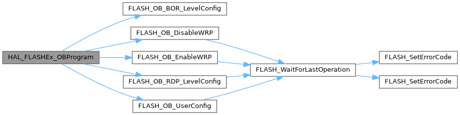
◆ HAL_FLASHEx_OBProgram()
| HAL_StatusTypeDef HAL_FLASHEx_OBProgram | ( | FLASH_OBProgramInitTypeDef * | pOBInit | ) |
Program option bytes.
- Parameters
-
pOBInit pointer to an FLASH_OBInitStruct structure that contains the configuration information for the programming.
- Return values
-
HAL Status
- Parameters
-
pOBInit pointer to an FLASH_OBInitStruct structure that contains the configuration information for the programming.
- Return values
-
HAL Status
Definition at line 314 of file stm32f4xx_hal_flash_ex.c.
Referenced by BOR_Set().

◆ HAL_FLASHEx_Unlock_Bank1()
| HAL_StatusTypeDef HAL_FLASHEx_Unlock_Bank1 | ( | void | ) |
Unlock the FLASH Bank1 control registers access.
- Return values
-
HAL Status
Definition at line 633 of file stm32h7xx_hal_flash_ex.c.
◆ HAL_FLASHEx_Unlock_Bank2()
| HAL_StatusTypeDef HAL_FLASHEx_Unlock_Bank2 | ( | void | ) |
Unlock the FLASH Bank2 control registers access.
- Return values
-
HAL Status
Definition at line 667 of file stm32h7xx_hal_flash_ex.c.