Functions | |
| static void | FLASH_MassErase (uint8_t VoltageRange, uint32_t Banks) |
| Full erase of FLASH memory sectors. | |
| void | FLASH_FlushCaches (void) |
| Flush the instruction and data caches. | |
| static HAL_StatusTypeDef | FLASH_OB_EnableWRP (uint32_t WRPSector, uint32_t Banks) |
| Enable the write protection of the desired bank1 or bank 2 sectors. | |
| static HAL_StatusTypeDef | FLASH_OB_DisableWRP (uint32_t WRPSector, uint32_t Banks) |
| Disable the write protection of the desired bank1 or bank 2 sectors. | |
| static HAL_StatusTypeDef | FLASH_OB_RDP_LevelConfig (uint8_t Level) |
| Set the read protection level. | |
| static HAL_StatusTypeDef | FLASH_OB_UserConfig (uint8_t Iwdg, uint8_t Stop, uint8_t Stdby) |
| Program the FLASH User Option Byte: IWDG_SW / RST_STOP / RST_STDBY. | |
| static HAL_StatusTypeDef | FLASH_OB_BOR_LevelConfig (uint8_t Level) |
| Set the BOR Level. | |
| static uint8_t | FLASH_OB_GetUser (void) |
| Return the FLASH User Option Byte value. | |
| static uint16_t | FLASH_OB_GetWRP (void) |
| Return the FLASH Write Protection Option Bytes value. | |
| static uint8_t | FLASH_OB_GetRDP (void) |
| Returns the FLASH Read Protection level. | |
| static uint8_t | FLASH_OB_GetBOR (void) |
| Returns the FLASH BOR level. | |
| static HAL_StatusTypeDef | FLASH_OB_EnablePCROP (uint32_t Sector) |
| Enable the read/write protection (PCROP) of the desired sectors. | |
| static HAL_StatusTypeDef | FLASH_OB_DisablePCROP (uint32_t Sector) |
| Disable the read/write protection (PCROP) of the desired sectors. | |
| static HAL_StatusTypeDef | FLASH_OB_EnablePCROP (uint32_t SectorBank1, uint32_t SectorBank2, uint32_t Banks) |
| Enable the read/write protection (PCROP) of the desired sectors of Bank 1 and/or Bank 2. | |
| static HAL_StatusTypeDef | FLASH_OB_DisablePCROP (uint32_t SectorBank1, uint32_t SectorBank2, uint32_t Banks) |
| Disable the read/write protection (PCROP) of the desired sectors of Bank 1 and/or Bank 2. | |
| static HAL_StatusTypeDef | FLASH_OB_BootConfig (uint8_t BootConfig) |
| Configure the Dual Bank Boot. | |
| HAL_StatusTypeDef | FLASH_WaitForLastOperation (uint32_t Timeout) |
| Wait for a FLASH operation to complete. | |
| void | FLASH_Erase_Sector (uint32_t Sector, uint8_t VoltageRange) |
| Erase the specified FLASH memory sector. | |
| static HAL_StatusTypeDef | FLASH_OB_EnableWRP (uint32_t WRPSector) |
| Enable the write protection of the desired bank1 or bank2 sectors. | |
| static HAL_StatusTypeDef | FLASH_OB_DisableWRP (uint32_t WRPSector) |
| Disable the write protection of the desired bank1 or bank 2 sectors. | |
| static HAL_StatusTypeDef | FLASH_OB_BootAddressConfig (uint32_t BootOption, uint32_t Address) |
| Configure Boot base address. | |
| static uint32_t | FLASH_OB_GetBootAddress (uint32_t BootOption) |
| Configure Boot base address. | |
| static HAL_StatusTypeDef | FLASH_OB_UserConfig (uint32_t Wwdg, uint32_t Iwdg, uint32_t Stop, uint32_t Stdby, uint32_t Iwdgstop, \ uint32_t Iwdgstdby, uint32_t NDBank, uint32_t NDBoot) |
| Program the FLASH User Option Byte: IWDG_SW / RST_STOP / RST_STDBY. | |
| static void | FLASH_MassErase (uint8_t VoltageRange) |
| Full erase of FLASH memory sectors. | |
| static HAL_StatusTypeDef | FLASH_OB_UserConfig (uint32_t Wwdg, uint32_t Iwdg, uint32_t Stop, uint32_t Stdby, uint32_t Iwdgstop, uint32_t Iwdgstdby) |
| Program the FLASH User Option Byte: IWDG_SW / RST_STOP / RST_STDBY. | |
| static HAL_StatusTypeDef | FLASH_OB_PCROP_Config (uint32_t PCROPSector) |
| Set the PCROP protection for sectors. | |
| static HAL_StatusTypeDef | FLASH_OB_PCROP_RDP_Config (uint32_t Pcrop_Rdp) |
| Set the PCROP_RDP value. | |
| static uint32_t | FLASH_OB_GetPCROP (void) |
| Return the FLASH PCROP Protection Option Bytes value. | |
| static uint32_t | FLASH_OB_GetPCROPRDP (void) |
| Return the FLASH PCROP_RDP option byte value. | |
| static void | FLASH_MassErase (uint32_t VoltageRange, uint32_t Banks) |
| Mass erase of FLASH memory. | |
| static void | FLASH_OB_GetWRP (uint32_t *WRPState, uint32_t *WRPSector, uint32_t Bank) |
| Get the write protection of the given bank 1 or bank 2 sectors. | |
| static void | FLASH_OB_RDPConfig (uint32_t RDPLevel) |
| Set the read protection level. | |
| static void | FLASH_OB_PCROPConfig (uint32_t PCROPConfig, uint32_t PCROPStartAddr, uint32_t PCROPEndAddr, uint32_t Banks) |
| Configure the Proprietary code readout protection of the desired addresses. | |
| static void | FLASH_OB_GetPCROP (uint32_t *PCROPConfig, uint32_t *PCROPStartAddr, uint32_t *PCROPEndAddr, uint32_t Bank) |
| Get the Proprietary code readout protection configuration on a given Bank. | |
| static void | FLASH_OB_BOR_LevelConfig (uint32_t Level) |
| Set the BOR Level. | |
| static void | FLASH_OB_UserConfig (uint32_t UserType, uint32_t UserConfig) |
| Program the FLASH User Option Byte. | |
| static void | FLASH_OB_BootAddConfig (uint32_t BootOption, uint32_t BootAddress0, uint32_t BootAddress1) |
| Set Boot address. | |
| static void | FLASH_OB_GetBootAdd (uint32_t *BootAddress0, uint32_t *BootAddress1) |
| Get Boot address. | |
| static void | FLASH_OB_SecureAreaConfig (uint32_t SecureAreaConfig, uint32_t SecureAreaStartAddr, uint32_t SecureAreaEndAddr, uint32_t Banks) |
| Set secure area configuration. | |
| static void | FLASH_OB_GetSecureArea (uint32_t *SecureAreaConfig, uint32_t *SecureAreaStartAddr, uint32_t *SecureAreaEndAddr, uint32_t Bank) |
| Get secure area configuration. | |
| static void | FLASH_CRC_AddSector (uint32_t Sector, uint32_t Bank) |
| Add a CRC sector to the list of sectors on which the CRC will be calculated. | |
| static void | FLASH_CRC_SelectAddress (uint32_t CRCStartAddr, uint32_t CRCEndAddr, uint32_t Bank) |
| Select CRC start and end memory addresses on which the CRC will be calculated. | |
| static void | FLASH_OB_CM4BootAddConfig (uint32_t BootOption, uint32_t BootAddress0, uint32_t BootAddress1) |
| Set CM4 Boot address. | |
| static void | FLASH_OB_GetCM4BootAdd (uint32_t *BootAddress0, uint32_t *BootAddress1) |
| Get CM4 Boot address. | |
| static void | FLASH_OB_OTP_LockConfig (uint32_t OTP_Block) |
| Configure the OTP Block Lock. | |
| static uint32_t | FLASH_OB_OTP_GetLock (void) |
| Get the OTP Block Lock. | |
| static void | FLASH_OB_SharedRAM_Config (uint32_t SharedRamConfig) |
| Configure the TCM / AXI Shared RAM. | |
| static uint32_t | FLASH_OB_SharedRAM_GetConfig (void) |
| Get the TCM / AXI Shared RAM configurtion. | |
| static void | FLASH_OB_CPUFreq_BoostConfig (uint32_t FreqBoost) |
| Configure the CPU Frequency Boost. | |
| static uint32_t | FLASH_OB_CPUFreq_GetBoost (void) |
| Get the CPU Frequency Boost state. | |
| void | FLASH_Erase_Sector (uint32_t Sector, uint32_t Banks, uint32_t VoltageRange) |
| Erase the specified FLASH memory sector. | |
Detailed Description
Function Documentation
◆ FLASH_CRC_AddSector()
|
static |
Add a CRC sector to the list of sectors on which the CRC will be calculated.
- Parameters
-
Sector Specifies the CRC sector number Bank Specifies the Bank
- Return values
-
None
Definition at line 1719 of file stm32h7xx_hal_flash_ex.c.
Referenced by HAL_FLASHEx_ComputeCRC().

◆ FLASH_CRC_SelectAddress()
|
static |
Select CRC start and end memory addresses on which the CRC will be calculated.
- Parameters
-
CRCStartAddr Specifies the CRC start address CRCEndAddr Specifies the CRC end address Bank Specifies the Bank
- Return values
-
None
Definition at line 1751 of file stm32h7xx_hal_flash_ex.c.
Referenced by HAL_FLASHEx_ComputeCRC().

◆ FLASH_Erase_Sector() [1/2]
| void FLASH_Erase_Sector | ( | uint32_t | Sector, |
| uint32_t | Banks, | ||
| uint32_t | VoltageRange | ||
| ) |
Erase the specified FLASH memory sector.
- Parameters
-
Sector FLASH sector to erase This parameter can be a value of FLASH Sectors Banks Banks to be erased This parameter can be one of the following values: - FLASH_BANK_1: Bank1 to be erased
- FLASH_BANK_2: Bank2 to be erased
- FLASH_BANK_BOTH: Bank1 and Bank2 to be erased
VoltageRange The device program/erase parallelism. This parameter can be one of the following values: - FLASH_VOLTAGE_RANGE_1 : Flash program/erase by 8 bits
- FLASH_VOLTAGE_RANGE_2 : Flash program/erase by 16 bits
- FLASH_VOLTAGE_RANGE_3 : Flash program/erase by 32 bits
- FLASH_VOLTAGE_RANGE_4 : Flash program/erase by 64 bits
- Return values
-
None
Definition at line 933 of file stm32h7xx_hal_flash_ex.c.

◆ FLASH_Erase_Sector() [2/2]
| void FLASH_Erase_Sector | ( | uint32_t | Sector, |
| uint8_t | VoltageRange | ||
| ) |
Erase the specified FLASH memory sector.
- Parameters
-
Sector FLASH sector to erase The value of this parameter depend on device used within the same series
VoltageRange The device voltage range which defines the erase parallelism.
This parameter can be one of the following values:- FLASH_VOLTAGE_RANGE_1: when the device voltage range is 1.8V to 2.1V, the operation will be done by byte (8-bit)
- FLASH_VOLTAGE_RANGE_2: when the device voltage range is 2.1V to 2.7V, the operation will be done by half word (16-bit)
- FLASH_VOLTAGE_RANGE_3: when the device voltage range is 2.7V to 3.6V, the operation will be done by word (32-bit)
- FLASH_VOLTAGE_RANGE_4: when the device voltage range is 2.7V to 3.6V + External Vpp, the operation will be done by double word (64-bit)
- Return values
-
None
Definition at line 637 of file stm32f4xx_hal_flash_ex.c.
Referenced by HAL_FLASH_IRQHandler(), HAL_FLASHEx_Erase(), and HAL_FLASHEx_Erase_IT().

◆ FLASH_FlushCaches()
| void FLASH_FlushCaches | ( | void | ) |
Flush the instruction and data caches.
- Return values
-
None
Definition at line 370 of file stm32f4xx_hal_flash_ex.c.
Referenced by HAL_FLASH_IRQHandler(), and HAL_FLASHEx_Erase().

◆ FLASH_MassErase() [1/3]
|
static |
Mass erase of FLASH memory.
- Parameters
-
VoltageRange The device program/erase parallelism. This parameter can be one of the following values: - FLASH_VOLTAGE_RANGE_1 : Flash program/erase by 8 bits
- FLASH_VOLTAGE_RANGE_2 : Flash program/erase by 16 bits
- FLASH_VOLTAGE_RANGE_3 : Flash program/erase by 32 bits
- FLASH_VOLTAGE_RANGE_4 : Flash program/erase by 64 bits
Banks Banks to be erased This parameter can be one of the following values: - FLASH_BANK_1: Bank1 to be erased
- FLASH_BANK_2: Bank2 to be erased
- FLASH_BANK_BOTH: Bank1 and Bank2 to be erased
- Return values
-
HAL Status
Definition at line 856 of file stm32h7xx_hal_flash_ex.c.

◆ FLASH_MassErase() [2/3]
|
static |
Full erase of FLASH memory sectors.
- Parameters
-
VoltageRange The device voltage range which defines the erase parallelism.
This parameter can be one of the following values:- VOLTAGE_RANGE_1: when the device voltage range is 1.8V to 2.1V, the operation will be done by byte (8-bit)
- VOLTAGE_RANGE_2: when the device voltage range is 2.1V to 2.7V, the operation will be done by half word (16-bit)
- VOLTAGE_RANGE_3: when the device voltage range is 2.7V to 3.6V, the operation will be done by word (32-bit)
- VOLTAGE_RANGE_4: when the device voltage range is 2.7V to 3.6V + External Vpp, the operation will be done by double word (64-bit)
- Return values
-
HAL Status
Definition at line 665 of file stm32f7xx_hal_flash_ex.c.
◆ FLASH_MassErase() [3/3]
|
static |
Full erase of FLASH memory sectors.
Mass erase of FLASH memory.
- Parameters
-
VoltageRange The device voltage range which defines the erase parallelism.
This parameter can be one of the following values:- FLASH_VOLTAGE_RANGE_1: when the device voltage range is 1.8V to 2.1V, the operation will be done by byte (8-bit)
- FLASH_VOLTAGE_RANGE_2: when the device voltage range is 2.1V to 2.7V, the operation will be done by half word (16-bit)
- FLASH_VOLTAGE_RANGE_3: when the device voltage range is 2.7V to 3.6V, the operation will be done by word (32-bit)
- FLASH_VOLTAGE_RANGE_4: when the device voltage range is 2.7V to 3.6V + External Vpp, the operation will be done by double word (64-bit)
Banks Banks to be erased This parameter can be one of the following values: - FLASH_BANK_1: Bank1 to be erased
- FLASH_BANK_2: Bank2 to be erased
- FLASH_BANK_BOTH: Bank1 and Bank2 to be erased
- Return values
-
HAL Status
- Parameters
-
VoltageRange The device voltage range which defines the erase parallelism.
This parameter can be one of the following values:- FLASH_VOLTAGE_RANGE_1: when the device voltage range is 1.8V to 2.1V, the operation will be done by byte (8-bit)
- FLASH_VOLTAGE_RANGE_2: when the device voltage range is 2.1V to 2.7V, the operation will be done by half word (16-bit)
- FLASH_VOLTAGE_RANGE_3: when the device voltage range is 2.7V to 3.6V, the operation will be done by word (32-bit)
- FLASH_VOLTAGE_RANGE_4: when the device voltage range is 2.7V to 3.6V + External Vpp, the operation will be done by double word (64-bit)
Banks Banks to be erased This parameter can be one of the following values: - FLASH_BANK_1: Bank1 to be erased
- Return values
-
None
Definition at line 591 of file stm32f4xx_hal_flash_ex.c.
Referenced by HAL_FLASHEx_Erase(), and HAL_FLASHEx_Erase_IT().

◆ FLASH_OB_BootAddConfig()
|
static |
Set Boot address.
- Parameters
-
BootOption Boot address option byte to be programmed, This parameter must be a value of FLASHEx OB BOOT OPTION (OB_BOOT_ADD0, OB_BOOT_ADD1 or OB_BOOT_ADD_BOTH) BootAddress0 Specifies the Boot Address 0 BootAddress1 Specifies the Boot Address 1
- Return values
-
HAL Status
Definition at line 1522 of file stm32h7xx_hal_flash_ex.c.
◆ FLASH_OB_BootAddressConfig()
|
static |
Configure Boot base address.
- Parameters
-
BootOption : specifies Boot base address depending from Boot pin = 0 or pin = 1 This parameter can be one of the following values: - OPTIONBYTE_BOOTADDR_0 : Boot address based when Boot pin = 0
- OPTIONBYTE_BOOTADDR_1 : Boot address based when Boot pin = 1
Address specifies Boot base address This parameter can be one of the following values: - OB_BOOTADDR_ITCM_RAM : Boot from ITCM RAM (0x00000000)
- OB_BOOTADDR_SYSTEM : Boot from System memory bootloader (0x00100000)
- OB_BOOTADDR_ITCM_FLASH : Boot from Flash on ITCM interface (0x00200000)
- OB_BOOTADDR_AXIM_FLASH : Boot from Flash on AXIM interface (0x08000000)
- OB_BOOTADDR_DTCM_RAM : Boot from DTCM RAM (0x20000000)
- OB_BOOTADDR_SRAM1 : Boot from SRAM1 (0x20010000)
- OB_BOOTADDR_SRAM2 : Boot from SRAM2 (0x2004C000)
- OPTIONBYTE_BOOTADDR_0 : Boot address based when Boot pin = 0
- Return values
-
HAL Status
Definition at line 958 of file stm32f7xx_hal_flash_ex.c.

◆ FLASH_OB_BootConfig()
|
static |
Configure the Dual Bank Boot.
- Note
- This function can be used only for STM32F42xxx/43xxx devices.
- Parameters
-
BootConfig specifies the Dual Bank Boot Option byte. This parameter can be one of the following values: - OB_Dual_BootEnabled: Dual Bank Boot Enable
- OB_Dual_BootDisabled: Dual Bank Boot Disabled
- Return values
-
None
Definition at line 829 of file stm32f4xx_hal_flash_ex.c.
Referenced by HAL_FLASHEx_AdvOBProgram().

◆ FLASH_OB_BOR_LevelConfig() [1/2]
|
static |
Set the BOR Level.
- Parameters
-
Level specifies the Option Bytes BOR Reset Level. This parameter can be one of the following values: - OB_BOR_LEVEL0: Reset level threshold is set to 1.6V
- OB_BOR_LEVEL1: Reset level threshold is set to 2.1V
- OB_BOR_LEVEL2: Reset level threshold is set to 2.4V
- OB_BOR_LEVEL3: Reset level threshold is set to 2.7V
- Return values
-
None
Definition at line 1490 of file stm32h7xx_hal_flash_ex.c.
◆ FLASH_OB_BOR_LevelConfig() [2/2]
|
static |
Set the BOR Level.
- Parameters
-
Level specifies the Option Bytes BOR Reset Level. This parameter can be one of the following values: - OB_BOR_LEVEL3: Supply voltage ranges from 2.7 to 3.6 V
- OB_BOR_LEVEL2: Supply voltage ranges from 2.4 to 2.7 V
- OB_BOR_LEVEL1: Supply voltage ranges from 2.1 to 2.4 V
- OB_BOR_OFF: Supply voltage ranges from 1.62 to 2.1 V
- Return values
-
HAL Status
Definition at line 1287 of file stm32f4xx_hal_flash_ex.c.
Referenced by HAL_FLASHEx_OBProgram().

◆ FLASH_OB_CM4BootAddConfig()
|
static |
Set CM4 Boot address.
- Parameters
-
BootOption Boot address option byte to be programmed, This parameter must be a value of FLASHEx OB BOOT OPTION (OB_BOOT_ADD0, OB_BOOT_ADD1 or OB_BOOT_ADD_BOTH) BootAddress0 Specifies the CM4 Boot Address 0. BootAddress1 Specifies the CM4 Boot Address 1.
- Return values
-
HAL Status
Definition at line 1588 of file stm32h7xx_hal_flash_ex.c.
◆ FLASH_OB_CPUFreq_BoostConfig()
|
static |
Configure the CPU Frequency Boost.
- Parameters
-
FreqBoost specifies the CPU Frequency Boost state. This parameter can be a value of FLASHEx OB CPUFREQ BOOST
- Return values
-
None
Definition at line 1839 of file stm32h7xx_hal_flash_ex.c.
◆ FLASH_OB_CPUFreq_GetBoost()
|
static |
Get the CPU Frequency Boost state.
- Return values
-
FreqBoost returns the CPU Frequency Boost state. This return value can be a value of FLASHEx OB CPUFREQ BOOST
Definition at line 1853 of file stm32h7xx_hal_flash_ex.c.
◆ FLASH_OB_DisablePCROP() [1/2]
|
static |
Disable the read/write protection (PCROP) of the desired sectors.
- Note
- This function can be used only for STM32F401xx devices.
- Parameters
-
Sector specifies the sector(s) to be read/write protected or unprotected. This parameter can be one of the following values: - OB_PCROP: A value between OB_PCROP_Sector0 and OB_PCROP_Sector5
- OB_PCROP_Sector_All
- Return values
-
HAL Status
Definition at line 1186 of file stm32f4xx_hal_flash_ex.c.
Referenced by HAL_FLASHEx_AdvOBProgram().


◆ FLASH_OB_DisablePCROP() [2/2]
|
static |
Disable the read/write protection (PCROP) of the desired sectors of Bank 1 and/or Bank 2.
- Note
- This function can be used only for STM32F42xxx/43xxx devices.
- Parameters
-
SectorBank1 specifies the sector(s) to be read/write protected or unprotected for bank1. This parameter can be one of the following values: - OB_PCROP: A value between OB_PCROP_SECTOR_0 and OB_PCROP_SECTOR_11
- OB_PCROP_SECTOR__All
SectorBank2 Specifies the sector(s) to be read/write protected or unprotected for bank2. This parameter can be one of the following values: - OB_PCROP: A value between OB_PCROP_SECTOR_12 and OB_PCROP_SECTOR_23
- OB_PCROP_SECTOR__All
Banks Disable PCROP protection on all the sectors for the specific bank This parameter can be one of the following values: - FLASH_BANK_1: WRP on all sectors of bank1
- FLASH_BANK_2: WRP on all sectors of bank2
- FLASH_BANK_BOTH: WRP on all sectors of bank1 & bank2
- Return values
-
HAL Status
Definition at line 933 of file stm32f4xx_hal_flash_ex.c.

◆ FLASH_OB_DisableWRP() [1/2]
|
static |
Disable the write protection of the desired bank1 or bank 2 sectors.
- Note
- When the memory read protection level is selected (RDP level = 1), it is not possible to program or erase the flash sector i if CortexM4
debug features are connected or boot code is executed in RAM, even if nWRPi = 1
- Parameters
-
WRPSector specifies the sector(s) to be write protected. This parameter can be one of the following values: - WRPSector: A value between OB_WRP_SECTOR_0 and OB_WRP_SECTOR_7 (for STM32F74xxx/STM32F75xxx devices) or a value between OB_WRP_SECTOR_0 and OB_WRP_SECTOR_11 (in Single Bank mode for STM32F76xxx/STM32F77xxx devices) or a value between OB_WRP_DB_SECTOR_0 and OB_WRP_DB_SECTOR_23 (in Dual Bank mode for STM32F76xxx/STM32F77xxx devices)
- OB_WRP_Sector_All
- WRPSector: A value between OB_WRP_SECTOR_0 and OB_WRP_SECTOR_7 (for STM32F74xxx/STM32F75xxx devices) or a value between OB_WRP_SECTOR_0 and OB_WRP_SECTOR_11 (in Single Bank mode for STM32F76xxx/STM32F77xxx devices) or a value between OB_WRP_DB_SECTOR_0 and OB_WRP_DB_SECTOR_23 (in Dual Bank mode for STM32F76xxx/STM32F77xxx devices)
- Return values
-
HAL Status
Definition at line 868 of file stm32f7xx_hal_flash_ex.c.

◆ FLASH_OB_DisableWRP() [2/2]
|
static |
Disable the write protection of the desired bank1 or bank 2 sectors.
Disable the write protection of the desired bank 1 sectors.
- Note
- When the memory read protection level is selected (RDP level = 1), it is not possible to program or erase the flash sector i if CortexM4
debug features are connected or boot code is executed in RAM, even if nWRPi = 1 -
Active value of nWRPi bits is inverted when PCROP mode is active (SPRMOD =1).
- Parameters
-
WRPSector specifies the sector(s) to be write protected. This parameter can be one of the following values: - WRPSector: A value between OB_WRP_SECTOR_0 and OB_WRP_SECTOR_23
- OB_WRP_Sector_All
- Note
- BANK2 starts from OB_WRP_SECTOR_12
- Parameters
-
Banks Disable write protection on all the sectors for the specific bank This parameter can be one of the following values: - FLASH_BANK_1: Bank1 to be erased
- FLASH_BANK_2: Bank2 to be erased
- FLASH_BANK_BOTH: Bank1 and Bank2 to be erased
- Return values
-
HAL Status
- Note
- When the memory read protection level is selected (RDP level = 1), it is not possible to program or erase the flash sector i if CortexM4
debug features are connected or boot code is executed in RAM, even if nWRPi = 1 -
Active value of nWRPi bits is inverted when PCROP mode is active (SPRMOD =1).
- Parameters
-
WRPSector specifies the sector(s) to be write protected. The value of this parameter depend on device used within the same series Banks Enable write protection on all the sectors for the specific bank This parameter can be one of the following values: - FLASH_BANK_1: WRP on all sectors of bank1
- Return values
-
HAL Status
- Parameters
-
WRPSector specifies the sector(s) to disable write protection. This parameter can be one of the following values: - WRPSector: A combination of FLASH_OB_WRP_SECTOR_0 to FLASH_OB_WRP_SECTOR_7 or FLASH_OB_WRP_SECTOR_All
Banks the specific bank to apply WRP sectors This parameter can be one of the following values: - FLASH_BANK_1: disable WRP on specified bank1 sectors
- FLASH_BANK_2: disable WRP on specified bank2 sectors
- FLASH_BANK_BOTH: disable WRP on both bank1 and bank2 specified sectors
- Return values
-
HAL FLASH State
Definition at line 768 of file stm32f4xx_hal_flash_ex.c.
Referenced by HAL_FLASHEx_OBProgram().

◆ FLASH_OB_EnablePCROP() [1/2]
|
static |
Enable the read/write protection (PCROP) of the desired sectors.
- Note
- This function can be used only for STM32F401xx devices.
- Parameters
-
Sector specifies the sector(s) to be read/write protected or unprotected. This parameter can be one of the following values: - OB_PCROP: A value between OB_PCROP_Sector0 and OB_PCROP_Sector5
- OB_PCROP_Sector_All
- Return values
-
HAL Status
Definition at line 1158 of file stm32f4xx_hal_flash_ex.c.
Referenced by HAL_FLASHEx_AdvOBProgram().

◆ FLASH_OB_EnablePCROP() [2/2]
|
static |
Enable the read/write protection (PCROP) of the desired sectors of Bank 1 and/or Bank 2.
- Note
- This function can be used only for STM32F42xxx/43xxx devices.
- Parameters
-
SectorBank1 Specifies the sector(s) to be read/write protected or unprotected for bank1. This parameter can be one of the following values: - OB_PCROP: A value between OB_PCROP_SECTOR_0 and OB_PCROP_SECTOR_11
- OB_PCROP_SECTOR__All
SectorBank2 Specifies the sector(s) to be read/write protected or unprotected for bank2. This parameter can be one of the following values: - OB_PCROP: A value between OB_PCROP_SECTOR_12 and OB_PCROP_SECTOR_23
- OB_PCROP_SECTOR__All
Banks Enable PCROP protection on all the sectors for the specific bank This parameter can be one of the following values: - FLASH_BANK_1: WRP on all sectors of bank1
- FLASH_BANK_2: WRP on all sectors of bank2
- FLASH_BANK_BOTH: WRP on all sectors of bank1 & bank2
- Return values
-
HAL Status
Definition at line 869 of file stm32f4xx_hal_flash_ex.c.

◆ FLASH_OB_EnableWRP() [1/2]
|
static |
Enable the write protection of the desired bank1 or bank2 sectors.
- Note
- When the memory read protection level is selected (RDP level = 1), it is not possible to program or erase the flash sector i if CortexM7
debug features are connected or boot code is executed in RAM, even if nWRPi = 1
- Parameters
-
WRPSector specifies the sector(s) to be write protected. This parameter can be one of the following values: - WRPSector: A value between OB_WRP_SECTOR_0 and OB_WRP_SECTOR_7 (for STM32F74xxx/STM32F75xxx devices) or a value between OB_WRP_SECTOR_0 and OB_WRP_SECTOR_11 (in Single Bank mode for STM32F76xxx/STM32F77xxx devices) or a value between OB_WRP_DB_SECTOR_0 and OB_WRP_DB_SECTOR_23 (in Dual Bank mode for STM32F76xxx/STM32F77xxx devices)
- OB_WRP_SECTOR_All
- Return values
-
HAL FLASH State
Definition at line 832 of file stm32f7xx_hal_flash_ex.c.

◆ FLASH_OB_EnableWRP() [2/2]
|
static |
Enable the write protection of the desired bank1 or bank 2 sectors.
Enable the write protection of the desired bank 1 sectors.
- Note
- When the memory read protection level is selected (RDP level = 1), it is not possible to program or erase the flash sector i if CortexM4
debug features are connected or boot code is executed in RAM, even if nWRPi = 1 -
Active value of nWRPi bits is inverted when PCROP mode is active (SPRMOD =1).
- Parameters
-
WRPSector specifies the sector(s) to be write protected. This parameter can be one of the following values: - WRPSector: A value between OB_WRP_SECTOR_0 and OB_WRP_SECTOR_23
- OB_WRP_SECTOR_All
- Note
- BANK2 starts from OB_WRP_SECTOR_12
- Parameters
-
Banks Enable write protection on all the sectors for the specific bank This parameter can be one of the following values: - FLASH_BANK_1: WRP on all sectors of bank1
- FLASH_BANK_2: WRP on all sectors of bank2
- FLASH_BANK_BOTH: WRP on all sectors of bank1 & bank2
- Return values
-
HAL FLASH State
- Note
- When the memory read protection level is selected (RDP level = 1), it is not possible to program or erase the flash sector i if CortexM4
debug features are connected or boot code is executed in RAM, even if nWRPi = 1 -
Active value of nWRPi bits is inverted when PCROP mode is active (SPRMOD =1).
- Parameters
-
WRPSector specifies the sector(s) to be write protected. The value of this parameter depend on device used within the same series Banks Enable write protection on all the sectors for the specific bank This parameter can be one of the following values: - FLASH_BANK_1: WRP on all sectors of bank1
- Return values
-
HAL Status
- Parameters
-
WRPSector specifies the sector(s) to be write protected. This parameter can be one of the following values: - WRPSector: A combination of OB_WRP_SECTOR_0 to OB_WRP_SECTOR_7 or OB_WRP_SECTOR_All
Banks the specific bank to apply WRP sectors This parameter can be one of the following values: - FLASH_BANK_1: enable WRP on specified bank1 sectors
- FLASH_BANK_2: enable WRP on specified bank2 sectors
- FLASH_BANK_BOTH: enable WRP on both bank1 and bank2 specified sectors
- Return values
-
HAL FLASH State
Definition at line 697 of file stm32f4xx_hal_flash_ex.c.
Referenced by HAL_FLASHEx_OBProgram().

◆ FLASH_OB_GetBootAdd()
|
static |
Get Boot address.
- Parameters
-
BootAddress0 Specifies the Boot Address 0. BootAddress1 Specifies the Boot Address 1.
- Return values
-
HAL Status
Definition at line 1560 of file stm32h7xx_hal_flash_ex.c.
◆ FLASH_OB_GetBootAddress()
|
static |
Configure Boot base address.
- Parameters
-
BootOption : specifies Boot base address depending from Boot pin = 0 or pin = 1 This parameter can be one of the following values: - OPTIONBYTE_BOOTADDR_0 : Boot address based when Boot pin = 0
- OPTIONBYTE_BOOTADDR_1 : Boot address based when Boot pin = 1
- OPTIONBYTE_BOOTADDR_0 : Boot address based when Boot pin = 0
- Return values
-
uint32_t Boot Base Address: - OB_BOOTADDR_ITCM_RAM : Boot from ITCM RAM (0x00000000)
- OB_BOOTADDR_SYSTEM : Boot from System memory bootloader (0x00100000)
- OB_BOOTADDR_ITCM_FLASH : Boot from Flash on ITCM interface (0x00200000)
- OB_BOOTADDR_AXIM_FLASH : Boot from Flash on AXIM interface (0x08000000)
- OB_BOOTADDR_DTCM_RAM : Boot from DTCM RAM (0x20000000)
- OB_BOOTADDR_SRAM1 : Boot from SRAM1 (0x20010000)
- OB_BOOTADDR_SRAM2 : Boot from SRAM2 (0x2004C000)
- OB_BOOTADDR_ITCM_RAM : Boot from ITCM RAM (0x00000000)
Definition at line 1042 of file stm32f7xx_hal_flash_ex.c.
◆ FLASH_OB_GetBOR()
|
static |
Returns the FLASH BOR level.
Get the BOR Level.
- Return values
-
uint8_t The FLASH BOR level: - OB_BOR_LEVEL3: Supply voltage ranges from 2.7 to 3.6 V
- OB_BOR_LEVEL2: Supply voltage ranges from 2.4 to 2.7 V
- OB_BOR_LEVEL1: Supply voltage ranges from 2.1 to 2.4 V
- OB_BOR_OFF : Supply voltage ranges from 1.62 to 2.1 V
The Option Bytes BOR Reset Level. This parameter can be one of the following values: - OB_BOR_LEVEL0: Reset level threshold is set to 1.6V
- OB_BOR_LEVEL1: Reset level threshold is set to 2.1V
- OB_BOR_LEVEL2: Reset level threshold is set to 2.4V
- OB_BOR_LEVEL3: Reset level threshold is set to 2.7V
Definition at line 1357 of file stm32f4xx_hal_flash_ex.c.
Referenced by HAL_FLASHEx_OBGetConfig().

◆ FLASH_OB_GetCM4BootAdd()
|
static |
Get CM4 Boot address.
- Parameters
-
BootAddress0 Specifies the CM4 Boot Address 0. BootAddress1 Specifies the CM4 Boot Address 1.
- Return values
-
HAL Status
Definition at line 1619 of file stm32h7xx_hal_flash_ex.c.
◆ FLASH_OB_GetPCROP() [1/2]
|
static |
Get the Proprietary code readout protection configuration on a given Bank.
- Parameters
-
PCROPConfig indicates if the PCROP area for the given Bank shall be erased or not when RDP level decreased from Level 1 to Level 0 or after a bank erase with protection removal PCROPStartAddr gives the start address of the Proprietary code readout protection of the bank PCROPEndAddr gives the end address of the Proprietary code readout protection of the bank Bank the specific bank to apply PCROP protection This parameter can be exclusively one of the following values: - FLASH_BANK_1: PCROP on specified bank1 area
- FLASH_BANK_2: PCROP on specified bank2 area
- FLASH_BANK_BOTH: is not allowed here
- Return values
-
None
Definition at line 1454 of file stm32h7xx_hal_flash_ex.c.
◆ FLASH_OB_GetPCROP() [2/2]
|
static |
Return the FLASH PCROP Protection Option Bytes value.
- Return values
-
uint32_t FLASH PCROP Protection Option Bytes value
Definition at line 1115 of file stm32f7xx_hal_flash_ex.c.
◆ FLASH_OB_GetPCROPRDP()
|
static |
Return the FLASH PCROP_RDP option byte value.
- Return values
-
uint32_t FLASH PCROP_RDP option byte value
Definition at line 1125 of file stm32f7xx_hal_flash_ex.c.
◆ FLASH_OB_GetRDP()
|
static |
Returns the FLASH Read Protection level.
Get the read protection level.
- Return values
-
FLASH ReadOut Protection Status: This parameter can be one of the following values: - OB_RDP_LEVEL_0: No protection
- OB_RDP_LEVEL_1: Read protection of the memory
- OB_RDP_LEVEL_2: Full chip protection
RDPLevel specifies the read protection level. This return value can be one of the following values: - OB_RDP_LEVEL_0: No protection
- OB_RDP_LEVEL_1: Read protection of the memory
- OB_RDP_LEVEL_2: Full chip protection
Definition at line 1329 of file stm32f4xx_hal_flash_ex.c.
Referenced by HAL_FLASHEx_OBGetConfig().

◆ FLASH_OB_GetSecureArea()
|
static |
Get secure area configuration.
- Parameters
-
SecureAreaConfig indicates if the secure area will be deleted or not when RDP level decreased from Level 1 to Level 0 or during a mass erase. SecureAreaStartAddr gives the secure area start address SecureAreaEndAddr gives the secure area end address Bank Specifies the Bank
- Return values
-
None
Definition at line 1686 of file stm32h7xx_hal_flash_ex.c.
◆ FLASH_OB_GetUser()
|
static |
Return the FLASH User Option Byte value.
- Return values
-
uint8_t FLASH User Option Bytes values: IWDG_SW(Bit0), RST_STOP(Bit1) and RST_STDBY(Bit2). The FLASH User Option Bytes values IWDG1_SW(Bit4), IWDG2_SW(Bit 5), nRST_STOP_D1(Bit 6), nRST_STDY_D1(Bit 7), FZ_IWDG_STOP(Bit 17), FZ_IWDG_SDBY(Bit 18), ST_RAM_SIZE(Bit[19:20]), SECURITY(Bit 21), BCM4(Bit 22), BCM7(Bit 23), nRST_STOP_D2(Bit 24), nRST_STDY_D2(Bit 25), IO_HSLV (Bit 29) and SWAP_BANK_OPT(Bit 31).
Return the FLASH User Option Byte value.
- Return values
-
The FLASH User Option Bytes values IWDG_SW(Bit4), nRST_STOP_D1(Bit 6), nRST_STDY_D1(Bit 7), FZ_IWDG_STOP(Bit 17), FZ_IWDG_SDBY(Bit 18), ST_RAM_SIZE(Bit[19:20]), SECURITY(Bit 21), IO_HSLV (Bit 29) and SWAP_BANK_OPT(Bit 31).
Definition at line 1305 of file stm32f4xx_hal_flash_ex.c.
Referenced by HAL_FLASHEx_OBGetConfig().

◆ FLASH_OB_GetWRP() [1/2]
|
static |
Get the write protection of the given bank 1 or bank 2 sectors.
- Parameters
-
WRPState gives the write protection state on the given bank. This parameter can be one of the following values: - WRPState: OB_WRPSTATE_DISABLE or OB_WRPSTATE_ENABLE
WRPSector gives the write protected sector(s) on the given bank . This parameter can be one of the following values: - WRPSector: A combination of FLASH_OB_WRP_SECTOR_0 to FLASH_OB_WRP_SECTOR_7 or FLASH_OB_WRP_SECTOR_All
Bank the specific bank to apply WRP sectors This parameter can be exclusively one of the following values: - FLASH_BANK_1: Get bank1 WRP sectors
- FLASH_BANK_2: Get bank2 WRP sectors
- FLASH_BANK_BOTH: note allowed in this functions
- Return values
-
HAL FLASH State
Definition at line 1064 of file stm32h7xx_hal_flash_ex.c.
◆ FLASH_OB_GetWRP() [2/2]
|
static |
Return the FLASH Write Protection Option Bytes value.
- Return values
-
uint16_t FLASH Write Protection Option Bytes value
Definition at line 1315 of file stm32f4xx_hal_flash_ex.c.
Referenced by HAL_FLASHEx_OBGetConfig().

◆ FLASH_OB_OTP_GetLock()
|
static |
Get the OTP Block Lock.
- Return values
-
OTP_Block specifies the OTP Block to lock. This return value can be a value of FLASH OTP blocks
Definition at line 1799 of file stm32h7xx_hal_flash_ex.c.
◆ FLASH_OB_OTP_LockConfig()
|
static |
Configure the OTP Block Lock.
- Parameters
-
OTP_Block specifies the OTP Block to lock. This parameter can be a value of FLASH OTP blocks
- Return values
-
None
Definition at line 1785 of file stm32h7xx_hal_flash_ex.c.
◆ FLASH_OB_PCROP_Config()
|
static |
Set the PCROP protection for sectors.
- Parameters
-
PCROPSector specifies the sector(s) to be PCROP protected. This parameter can be one of the following values: - OB_PCROP_SECTOR_x: A value between OB_PCROP_SECTOR_0 and OB_PCROP_SECTOR_7
- OB_PCROP_SECTOR_ALL
- Return values
-
HAL Status
Definition at line 1069 of file stm32f7xx_hal_flash_ex.c.

◆ FLASH_OB_PCROP_RDP_Config()
|
static |
Set the PCROP_RDP value.
- Parameters
-
Pcrop_Rdp specifies the PCROP_RDP bit value.
- Return values
-
HAL Status
Definition at line 1093 of file stm32f7xx_hal_flash_ex.c.

◆ FLASH_OB_PCROPConfig()
|
static |
Configure the Proprietary code readout protection of the desired addresses.
- Note
- To configure the PCROP options, the option lock bit OPTLOCK must be cleared with the call of the HAL_FLASH_OB_Unlock() function.
- To validate the PCROP options, the option bytes must be reloaded through the call of the HAL_FLASH_OB_Launch() function.
- Parameters
-
PCROPConfig specifies if the PCROP area for the given Bank shall be erased or not when RDP level decreased from Level 1 to Level 0, or after a bank erase with protection removal This parameter must be a value of - FLASHEx_OB_PCROP_RDP enumeration
PCROPStartAddr specifies the start address of the Proprietary code readout protection This parameter can be an address between begin and end of the bank PCROPEndAddr specifies the end address of the Proprietary code readout protection This parameter can be an address between PCROPStartAddr and end of the bank Banks the specific bank to apply PCROP protection This parameter can be one of the following values: - FLASH_BANK_1: PCROP on specified bank1 area
- FLASH_BANK_2: PCROP on specified bank2 area
- FLASH_BANK_BOTH: PCROP on specified bank1 and bank2 area (same config will be applied on both banks)
- Return values
-
None
Definition at line 1405 of file stm32h7xx_hal_flash_ex.c.
◆ FLASH_OB_RDP_LevelConfig()
|
static |
Set the read protection level.
- Parameters
-
Level specifies the read protection level. This parameter can be one of the following values: - OB_RDP_LEVEL_0: No protection
- OB_RDP_LEVEL_1: Read protection of the memory
- OB_RDP_LEVEL_2: Full chip protection
- Note
- WARNING: When enabling OB_RDP level 2 it's no more possible to go back to level 1 or 0
- Return values
-
HAL Status
Definition at line 1218 of file stm32f4xx_hal_flash_ex.c.
Referenced by HAL_FLASHEx_OBProgram().

◆ FLASH_OB_RDPConfig()
|
static |
Set the read protection level.
- Note
- To configure the RDP level, the option lock bit OPTLOCK must be cleared with the call of the HAL_FLASH_OB_Unlock() function.
- To validate the RDP level, the option bytes must be reloaded through the call of the HAL_FLASH_OB_Launch() function.
- !!! Warning : When enabling OB_RDP level 2 it's no more possible to go back to level 1 or 0 !!!
- Parameters
-
RDPLevel specifies the read protection level. This parameter can be one of the following values: - OB_RDP_LEVEL_0: No protection
- OB_RDP_LEVEL_1: Read protection of the memory
- OB_RDP_LEVEL_2: Full chip protection
- Return values
-
HAL status
Definition at line 1110 of file stm32h7xx_hal_flash_ex.c.
◆ FLASH_OB_SecureAreaConfig()
|
static |
Set secure area configuration.
- Parameters
-
SecureAreaConfig specify if the secure area will be deleted or not when RDP level decreased from Level 1 to Level 0 or during a mass erase. SecureAreaStartAddr Specifies the secure area start address SecureAreaEndAddr Specifies the secure area end address Banks the specific bank to apply Security protection This parameter can be one of the following values: - FLASH_BANK_1: Secure area on specified bank1 area
- FLASH_BANK_2: Secure area on specified bank2 area
- FLASH_BANK_BOTH: Secure area on specified bank1 and bank2 area (same config will be applied on both banks)
- Return values
-
None
Definition at line 1644 of file stm32h7xx_hal_flash_ex.c.
◆ FLASH_OB_SharedRAM_Config()
|
static |
Configure the TCM / AXI Shared RAM.
- Parameters
-
SharedRamConfig specifies the Shared RAM configuration. This parameter can be a value of FLASHEx OB TCM AXI SHARED
- Return values
-
None
Definition at line 1812 of file stm32h7xx_hal_flash_ex.c.
◆ FLASH_OB_SharedRAM_GetConfig()
|
static |
Get the TCM / AXI Shared RAM configurtion.
- Return values
-
SharedRamConfig returns the TCM / AXI Shared RAM configuration. This return value can be a value of FLASHEx OB TCM AXI SHARED
Definition at line 1826 of file stm32h7xx_hal_flash_ex.c.
◆ FLASH_OB_UserConfig() [1/4]
|
static |
Program the FLASH User Option Byte.
- Note
- To configure the user option bytes, the option lock bit OPTLOCK must be cleared with the call of the HAL_FLASH_OB_Unlock() function.
- To validate the user option bytes, the option bytes must be reloaded through the call of the HAL_FLASH_OB_Launch() function.
- Parameters
-
UserType The FLASH User Option Bytes to be modified : a combination of FLASHEx OB USER Type UserConfig The FLASH User Option Bytes values: IWDG1_SW(Bit4), IWDG2_SW(Bit 5), nRST_STOP_D1(Bit 6), nRST_STDY_D1(Bit 7), FZ_IWDG_STOP(Bit 17), FZ_IWDG_SDBY(Bit 18), ST_RAM_SIZE(Bit[19:20]), SECURITY(Bit 21), BCM4(Bit 22), BCM7(Bit 23), nRST_STOP_D2(Bit 24), nRST_STDY_D2(Bit 25), IO_HSLV (Bit 29) and SWAP_BANK_OPT(Bit 31).
- Return values
-
HAL status
Program the FLASH User Option Byte.
- Note
- To configure the user option bytes, the option lock bit OPTLOCK must be cleared with the call of the HAL_FLASH_OB_Unlock() function.
- To validate the user option bytes, the option bytes must be reloaded through the call of the HAL_FLASH_OB_Launch() function.
- Parameters
-
UserType The FLASH User Option Bytes to be modified : a combination of - FLASHEx_OB_USER_Type
UserConfig The FLASH User Option Bytes values: IWDG_SW(Bit4), nRST_STOP_D1(Bit 6), nRST_STDY_D1(Bit 7), FZ_IWDG_STOP(Bit 17), FZ_IWDG_SDBY(Bit 18), ST_RAM_SIZE(Bit[19:20]), SECURITY(Bit 21), IO_HSLV (Bit 29) and SWAP_BANK_OPT(Bit 31).
- Return values
-
HAL status
Definition at line 1183 of file stm32h7xx_hal_flash_ex.c.
◆ FLASH_OB_UserConfig() [2/4]
|
static |
Program the FLASH User Option Byte: IWDG_SW / RST_STOP / RST_STDBY.
- Parameters
-
Wwdg Selects the IWDG mode This parameter can be one of the following values: - OB_WWDG_SW: Software WWDG selected
- OB_WWDG_HW: Hardware WWDG selected
Iwdg Selects the WWDG mode This parameter can be one of the following values: - OB_IWDG_SW: Software IWDG selected
- OB_IWDG_HW: Hardware IWDG selected
Stop Reset event when entering STOP mode. This parameter can be one of the following values: - OB_STOP_NO_RST: No reset generated when entering in STOP
- OB_STOP_RST: Reset generated when entering in STOP
Stdby Reset event when entering Standby mode. This parameter can be one of the following values: - OB_STDBY_NO_RST: No reset generated when entering in STANDBY
- OB_STDBY_RST: Reset generated when entering in STANDBY
Iwdgstop Independent watchdog counter freeze in Stop mode. This parameter can be one of the following values: - OB_IWDG_STOP_FREEZE: Freeze IWDG counter in STOP
- OB_IWDG_STOP_ACTIVE: IWDG counter active in STOP
Iwdgstdby Independent watchdog counter freeze in standby mode. This parameter can be one of the following values: - OB_IWDG_STDBY_FREEZE: Freeze IWDG counter in STANDBY
- OB_IWDG_STDBY_ACTIVE: IWDG counter active in STANDBY
NDBank Flash Single Bank mode enabled. This parameter can be one of the following values: - OB_NDBANK_SINGLE_BANK: enable 256 bits mode (Flash is a single bank)
- OB_NDBANK_DUAL_BANK: disable 256 bits mode (Flash is a dual bank in 128 bits mode)
NDBoot Flash Dual boot mode disable. This parameter can be one of the following values: - OB_DUAL_BOOT_DISABLE: Disable Dual Boot
- OB_DUAL_BOOT_ENABLE: Enable Dual Boot
- Return values
-
HAL Status
Definition at line 602 of file stm32f7xx_hal_flash_ex.c.

◆ FLASH_OB_UserConfig() [3/4]
|
static |
Program the FLASH User Option Byte: IWDG_SW / RST_STOP / RST_STDBY.
- Parameters
-
Wwdg Selects the IWDG mode This parameter can be one of the following values: - OB_WWDG_SW: Software WWDG selected
- OB_WWDG_HW: Hardware WWDG selected
Iwdg Selects the WWDG mode This parameter can be one of the following values: - OB_IWDG_SW: Software IWDG selected
- OB_IWDG_HW: Hardware IWDG selected
Stop Reset event when entering STOP mode. This parameter can be one of the following values: - OB_STOP_NO_RST: No reset generated when entering in STOP
- OB_STOP_RST: Reset generated when entering in STOP
Stdby Reset event when entering Standby mode. This parameter can be one of the following values: - OB_STDBY_NO_RST: No reset generated when entering in STANDBY
- OB_STDBY_RST: Reset generated when entering in STANDBY
Iwdgstop Independent watchdog counter freeze in Stop mode. This parameter can be one of the following values: - OB_IWDG_STOP_FREEZE: Freeze IWDG counter in STOP
- OB_IWDG_STOP_ACTIVE: IWDG counter active in STOP
Iwdgstdby Independent watchdog counter freeze in standby mode. This parameter can be one of the following values: - OB_IWDG_STDBY_FREEZE: Freeze IWDG counter in STANDBY
- OB_IWDG_STDBY_ACTIVE: IWDG counter active in STANDBY
- Return values
-
HAL Status
Definition at line 771 of file stm32f7xx_hal_flash_ex.c.

◆ FLASH_OB_UserConfig() [4/4]
|
static |
Program the FLASH User Option Byte: IWDG_SW / RST_STOP / RST_STDBY.
- Parameters
-
Iwdg Selects the IWDG mode This parameter can be one of the following values: - OB_IWDG_SW: Software IWDG selected
- OB_IWDG_HW: Hardware IWDG selected
Stop Reset event when entering STOP mode. This parameter can be one of the following values: - OB_STOP_NO_RST: No reset generated when entering in STOP
- OB_STOP_RST: Reset generated when entering in STOP
Stdby Reset event when entering Standby mode. This parameter can be one of the following values: - OB_STDBY_NO_RST: No reset generated when entering in STANDBY
- OB_STDBY_RST: Reset generated when entering in STANDBY
- Return values
-
HAL Status
Definition at line 1252 of file stm32f4xx_hal_flash_ex.c.
Referenced by HAL_FLASHEx_OBProgram().


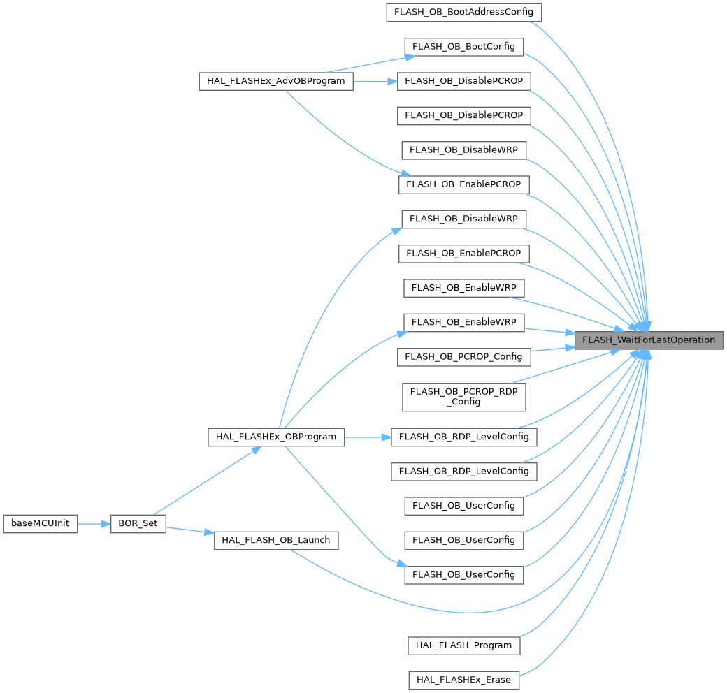
◆ FLASH_WaitForLastOperation()
|
extern |
Wait for a FLASH operation to complete.
- Parameters
-
Timeout maximum flash operationtimeout
- Return values
-
HAL Status
Definition at line 569 of file stm32f4xx_hal_flash.c.
Referenced by FLASH_OB_BootAddressConfig(), FLASH_OB_BootConfig(), FLASH_OB_DisablePCROP(), FLASH_OB_DisablePCROP(), FLASH_OB_DisableWRP(), FLASH_OB_DisableWRP(), FLASH_OB_EnablePCROP(), FLASH_OB_EnablePCROP(), FLASH_OB_EnableWRP(), FLASH_OB_EnableWRP(), FLASH_OB_PCROP_Config(), FLASH_OB_PCROP_RDP_Config(), FLASH_OB_RDP_LevelConfig(), FLASH_OB_RDP_LevelConfig(), FLASH_OB_UserConfig(), FLASH_OB_UserConfig(), FLASH_OB_UserConfig(), HAL_FLASH_OB_Launch(), HAL_FLASH_Program(), and HAL_FLASHEx_Erase().