Sudo wrote:As far as VR simulation, the only problem I see with the VR simulation is that the signal bandwidth needs to be MaxRPM*Teeths*Resolution, which is most likely in the MHz range. I highly doubt the DSO can do this. I am not sure if its worth trying to simulate a VR signal using circuitry only. A parallel DAC may work, but the GPIO have to be fast enough to drive a 2 times the speed of the signal. Anyone know how fast the STM32 can go with the GPIO? It seems we would be pushing the limit of a MCU. An FPGA driving a parallel DAC can certainly achieve this without a problem, but it is more costly. At the end, it really seems a dc motor with a wheel seems to be much simpler and more a realistic stimulus. Maybe we can hack junk hard drives to do this.

Assume a 36 tooth wheel at 10000 RPM: 360000 teeth per minute / 60 seconds = 6000 teeth per second = 6KHz signal / 12KHz if you're counting rising and falling edges. MSP430G2553 @ 16MHz core clock (little brother to the F5529 in the LP I mentioned) can toggle pins well in excess of 50KHz; I suspect STMF32 can do at least that. So, toggling a couple pins isn't such the issue it seems. I mean, consider that these processors have instructions that are single-cycle, meaning it takes one clock cycle to do the job. At 16MHz, that's 16 million cycles per second; STM32 @ 80+ MHz? See what I mean?
And if you're not comfortable with the F5529LP, there's always the
TM4C123GXL running an 80MHz Cortex-M4 similar to the STM32F4, which is pin-compatible with the stimulator board I posted. Both are $12.99 USD.
Anyhow, the biggest problems I see with generating the actual VR signal are: many VR's are dual-ended meaning it has a negative voltage component (some have one wire tied to ground so are single-ended); the voltages increase with frequency. When you're stuck with a 0-3v or 0-5v signal, getting a signal that can be +20/-20 or even more isn't so easy. LM1918 can handle this somewhat but MAX9926 and related are most often used with 0v crossing so if the voltage never goes below 0v, it never crosses- there are options for that too but it's a different circuit.
However, I do have one minor concern with using DACs now that I thought about it more. Most likely the ECU have their ADC reference set to the rail. That means, it is possible that if the ECU rail fluctuates, we can induce noises and/or offsets into the input relative to the ECU rail. I am not sure if this is critical or even an issue, but basically we are betting on the fact that ECU rails is rock solid, which may or may not be the case. But then again, this is just the stimulator board. Accuracy doesn't seem critical for this application. But it is just a thought to keep in mind.
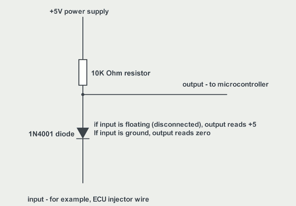
A workaround to an MCU with hard-wired ADCREF is possible. Divide your sensors' 5v rail and sensor inputs with resistor dividers or op-amps so that they are below the maximum voltage the ADC can sample, then sample the 5v rail along with the sensors. If you have a 12 bit ADC with 3v reference, you have potential resolution of better than 0.01v (3v / 4096 steps = 0.00732v per step) though you'll be limited to around 3400 steps since the voltage being sampled will not get near 3v unless you have a serious problem; a 2.5v internal reference is possible but if the 5v rail or any sensor goes above 5v you'll saturate the ADC.
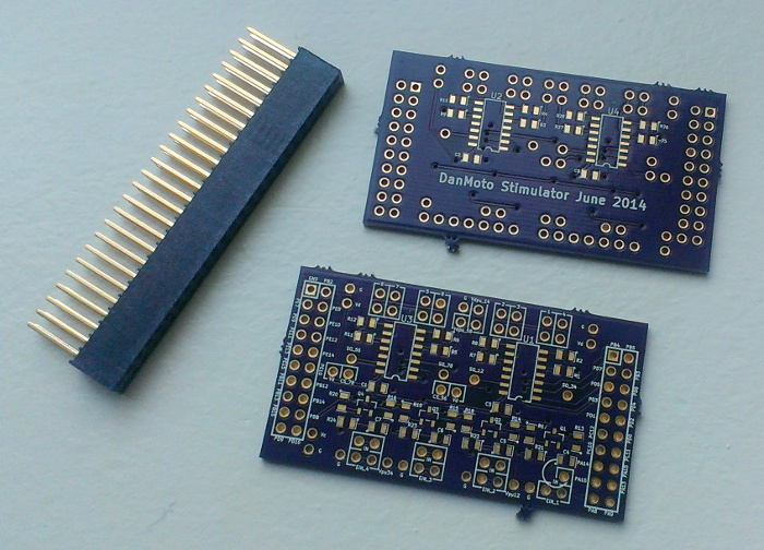
It's hard to see but that's what I've planned on the board I posted. Each pot has a pair of 100K resistors arranged to divide the voltage in half. The top plane is ground, bottom is 5v. Header SV1/Pin11 is connected to the 5v plane along with all the pots and has a pair of 100K resistors arranged as dividers and SV1/Pin13 is ADC0 on the MCU. SV1/Pin14-17 are also ADC (ADC1-ADC4 actually) as well. What I haven't done is permit a way to disconnect the pots from the circuits so external sensors can be connected for logging instead of stimulating, but that's a trivial modification to the board, nor have I worked out a similar thing for cam / crank signal logging. It is in the plan to do so though, probably a DIP slider or something to choose stimulator or logger with the firmware responding appropriately.

Pins 1 & 2 on the CAM_CRANK_OUT terminals are connected to the 5v plane and GND plane, respectively. Pins 3 & 4 care CAM and CRANK signal outputs with LED's and current limiting resistors.
The F5529LP board itself provides 5v for USB ICDI and other related operations and normally has that connected between the debug interface and MCU but it can be disconnected which permits having two different 5v rails- one for USB connectivity when needed and one external 5v source. The only caveat is that the GND between the two sections of the LP are connected so if the GND potentials are different between the external and USB side there can be problems, but in the situation where the engine is in the vehicle and there are no other connections such as through a battery charger or such, the "floating" ground of the vehicle will equal the ground on the board so no problem there.
You can lead the horticulture but you can't make them think.


 (and a capacitor to GND)